
Leave A Message
If you are interested in our products and want to know more details,please leave a message here,we will reply you as soon as we can.


Open Magnetic Path EMI Signatures: How Leakage Fields Show Up on EMC Scans
Open magnetic path EMI signatures appear when flux is not confined inside a high-permeability closed core—because of gapped inductors, poorly canceled windings, rod-like open structures, or leakage from CMCs—and that escaping field couples into cables, PCB loops, and chamber antennas.
On EMC scans you often see broadband or harmonic-rich elevations that change dramatically when you move a near-field probe around the magnetics or slightly relocate a harness. Fixing capacitors alone rarely solves it: you need magnetic path control, winding symmetry, layout distance, and sometimes shields—plus the right nanocrystalline or ferrite core strategy for the filter role.
Start from the CMC selection guide when the part is truly CM duty.
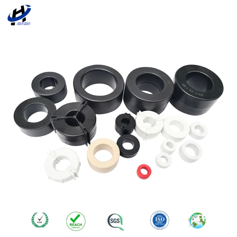
Cased closed-path CMCs: flux stays in the core. Open-path or poorly canceled turns leak onto nearby loops.
A toroidal high-μ nanocrystalline CMC aims for a closed magnetic path: common-mode ampere-turns drive flux in the core; differential current largely cancels. An open path (intentional gap, rod core, incomplete cancellation, large leakage) stores or leaks energy outside the core volume.
Leakage fields are useful (transformer isolation, some sensors) and harmful (EMI, heating of nearby metal, acoustic vibration). EMC labs see the harmful side as conducted noise that looks immune to Y-cap tweaks, radiated hotspots near magnetics, and failures that appear only with production cable routing.
| Observation | Suggests |
|---|---|
| Near-field probe peaks at gap or rod ends | Fringing / open path radiation |
| EMI changes when rotating a toroid CMC | Leakage / winding asymmetry |
| Fail band tracks f_sw harmonics | Switching magnetics coupling |
| Touching chassis near inductor shifts plot | Field into structure currents |
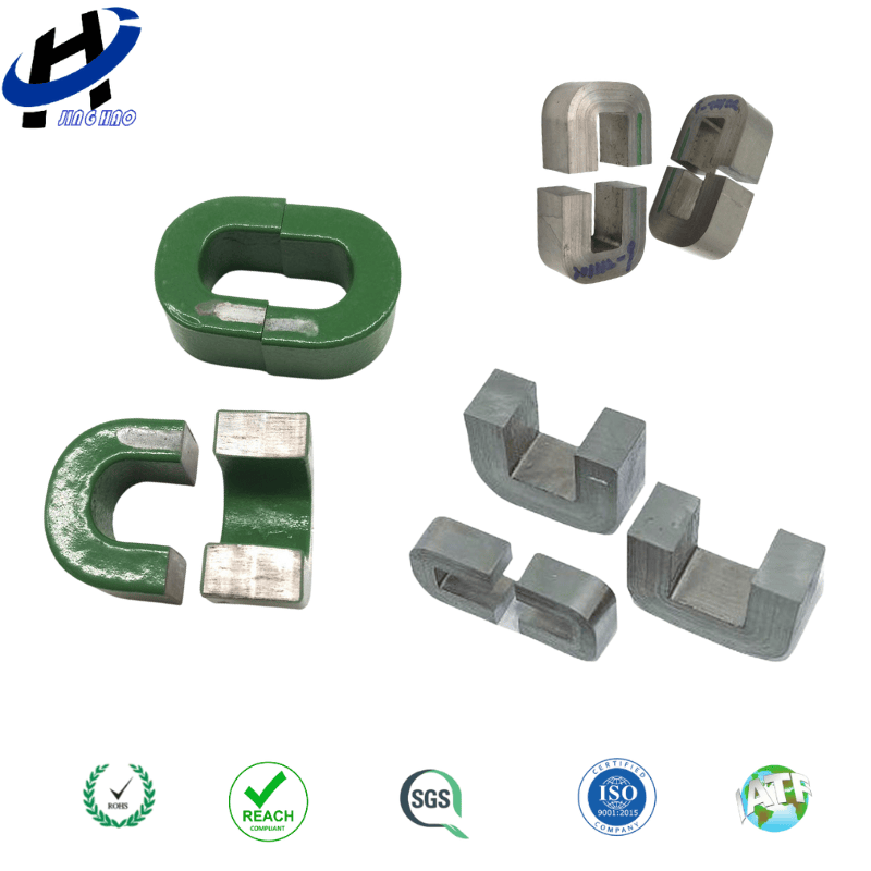
Cut / gapped cores: the open magnetic path is intentional for energy storage—and it is also where EMI probes light up.
CM vs DM roles. CMCs have intentional or parasitic leakage inductance that can help differential filtering—but excess leakage and poor winding symmetry radiate and convert modes. High-μ nanocrystalline CMCs (μ often ≈ 80,000–190,000 for CMC grades) are excellent closed-path CM impedances when wound correctly; they are not automatic EMC insurance if lead dress creates large loops.
Gapped DM inductors must leak by design. That fringe is where copper hotspots and EMI pickup coexist—see the fringing loss notes. Treat gap orientation as an EMC orientation problem, not only a thermal one.
Reading the scan like a magnetics engineer
This order prevents expensive core swaps when a 20 mm cable move was the real fix.
Magnetic design. Prefer closed-path CMCs for CM noise; use nanocrystalline when high current + strong low-frequency CM impedance is needed (Bs ~1.25 T class headroom vs ferrite ~0.4 T). For gapped DM parts, minimize unnecessary loop area and keep fringe away from sensitive nets. Avoid treating open rods as filters next to long cables without a shielding strategy.
Layout. Short, tight CMC lead pairs. Keep noisy switch nodes away from magnetics that can re-radiate. Mind return paths under inductors on multilayer PCBs.
Mechanical. Gap mark orientation standardized in assembly. Metal brackets can be useful shields or accidental shorted turns—validate.
System. Cable common-mode chokes at panel entry when cabinet coupling dominates. Keep grounding philosophy consistent with safety and EMC.
Ferrite may derate as temperatures approach the ~100–120°C discussion zone; nanocrystalline Curie ~570°C and finished assemblies often discussed from about -40°C to +140°C change the thermal EMI story. Neither material removes the need for closed-path thinking. An open-path ferrite and an open-path nanocrystalline can both fail radiated tests if layout ignores leakage.
Dongguan JH Amorphous supports OEM/ODM cores for CMCs and inductors under ISO9001:2015 and IATF 16949. Match closed-path CMC grades vs inductor grades so EMI roles stay clear.
| Approach | When it helps | When it fails |
|---|---|---|
| More X/Y capacitors | True CM/DM impedance gaps | Leakage coupling / loop antennas |
| Snubbers | Switching edges | Not a substitute for open-path control |
| Shield cans | Local radiated | Thermal & capacitive side effects |
| Closed-path CMC upgrade | High CM current, hot, LF EMI | Wrong if problem is DM gap radiation only |
| Cable routing / twist | Harness pickup | Ignores on-board fringe |
Mode conversion. Leakage and imbalance convert differential switching energy into common-mode currents on cables. That is why a “DM-only” inductor problem becomes a conducted CM fail on the LISN. Symmetry, tightly paired returns, and correct CMC placement after the noisy node are essential.
Pre-compliance checklist.
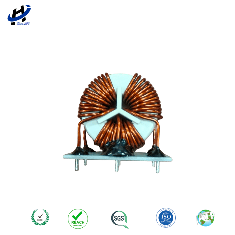
Wound toroids on the bench: lead dress and proximity to harnesses often move the EMC plot more than another capacitor.
Higher μ helps confine flux in a closed core for CM magnetization, but winding asymmetry and external loops still radiate. Gapped inductors will always fringe.
Magnetically unwise—different grades and purposes. See high-μ vs low-μ datasheet guidance.
Harnesses form antennas and return paths that lab pigtails omit. Leakage fields need those antennas to show up.
Fail bands, topology, currents, photos of magnetics orientation, and whether the part is CM or DM duty.
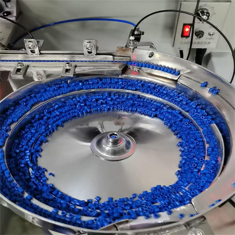
High-volume casing lines: mechanical consistency of the case also affects leakage and mounting geometry.
If an EMC plot seems to blame the toroid, send fail bands and magnetics photos to julia@amorphousoem.com — www.amorphousoem.com.
 Room 701, Jizhou Tongde Street 45, Shijie Town, Dongguan City, Guangdong Province, China
 +86-180 2701 0075
 sales@amorphousoem.com


 IPv6 network supported |
Sitemap
|
XML
|
blogs
|
Privacy Policy
IPv6 network supported |
Sitemap
|
XML
|
blogs
|
Privacy Policy