Sep 23, 2026
Why is the copper next to the gap always the hotspot?
Air-gap fringing loss appears when the magnetic field bulges out of a discrete gap and cuts nearby copper, inducing extra eddy-current heating. That is why thermal cameras often show winding hotspots immediately adjacent to the gap—even when average current density looks safe. Reduce the problem by keeping copper out of the strongest fringe, using spacer/coil architectures that distance the first turns, considering distributed or carefully shaped gaps, and verifying both loss and inductance under DC bias. Material choice (ferrite, amorphous, nanocrystalline) still matters for Bs and temperature, but winding geometry next to the gap frequently dominates local hotspots.
Why fringing exists and where it heats
An air gap stores energy by lowering effective permeability and linearizing AL under DC bias. The field does not stop abruptly at the gap edges: flux fringes into the winding window.
Consequences: local H and B outside the intended gap volume; AC field components cutting copper strands → eddy losses that scale badly with frequency and strand diameter; proximity-effect aggravation in nearby layers; mechanical forces that contribute to acoustic noise. For OEM power inductors in PFC stages, DC–DC bricks, and differential-mode chokes, fringing is everyday gapped design—not a corner case.
LocationWhy it runs hotMitigation theme
Turns hugging gap facesStrongest fringe cuts copperKeep clearance; use slot bobbins
Inner layer near gap on cut toroidConcentrated bulgeOffset winding, spacer
Thick Litz bundle in fringeStrand eddySmaller strands, move bundle
PCB copper under gapped ER/PQField into planeCutouts, distance
Fringing loss vs classic copper I²R: Design reviews sometimes blame “not enough copper” when IR drop is fine but the hotspot is brutal. Split the budget: (1) DC I²R from I_rms and resistance; (2) skin and proximity in the winding volume generally; (3) fringing-induced eddy localized where gap flux escapes. Item (3) can dominate a small region, raising local temperature enough to discolor enamel while average winding rise looks acceptable.
Rule-of-thumb notes (refine with FEA or experiment): fringing influence extends on the order of the gap length into the window—treat “several gap lengths” as a keep-out intuition. Higher f_sw and larger strand diameter in the fringe make eddy heating worse. Increasing gap to hold L under bias can improve magnetic linearity yet worsen fringe heating—trade explicitly.
Nanocrystalline and amorphous gapped cores used for high-current inductors—including PFC inductor cores—can run substantial AC flux. Bs headroom (~1.25 T class for iron-based nanocrystalline vs ~0.4 T ferrite) helps size, but copper next to the gap still needs respect. Treat core shape and gap method as the technical distinction—not casual shape nicknames.
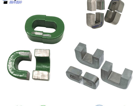
Cut C-cores make the gap explicit: fringing fields leave the cut faces and heat nearby copper.
How to place windings on gapped cores
Cut / gapped toroid: Identify gap location on the finished core. Leave a copper-free sector around the gap when the design allows. Start winding away from the gap; use tape or spacer to enforce distance. Prefer Litz appropriate for f_sw, but do not park a thick bundle in the fringe to fill the window. For production, document winding start angle relative to the gap mark so every operator repeats the thermal result.
Bobbin cores (PQ, E, ER): Use coil geometries that recess the first winding layer from the gap centerline. Watch foil windings: wide foils are efficient for DC but can act as eddy sails in fringe—slotting or distancing may be required. Thermal vias and potting help only if heat can leave; they do not remove the eddy source.
Distributed gap approaches: Distributed gaps reduce peak fringe intensity compared with one large discrete gap, often improving copper temperature at the cost of different loss and cost structures. Evaluate on your f_sw and current; do not assume “distributed always cooler” without measurement.
Dongguan JH Amorphous supplies OEM/ODM nanocrystalline and amorphous cores (ISO9001:2015, IATF 16949). For inductor grades we emphasize AL vs DC bias, loss orientation, and manufacturing marks that help winding houses avoid the gap hotspot.
Product mix showing cut cores beside closed toroids—gap policy belongs in the RFQ, not as an afterthought.
Design workflow and production drift
Set L(I) requirement—define I_sat and I_rms.
Choose gap / effective μ strategy—discrete vs distributed.
Estimate copper loss without fringe; then add experimental margin or FEA for the gap region.
Prototype with a thermal camera focused on gap-adjacent copper.
Iterate winding distance and stranding before enlarging the core as a first move.
Re-check EMI and acoustics—gap and winding changes affect leakage and noise (and can feed inductor whistle if ΔB sits in the audio band).
LeverProsCons
Increase clearance to gapFast, low tooling costMay reduce turns window
Finer Litz in fringe zoneCuts eddy in hotspotCost, fill factor
Split/distribute gapLower peak fringeProcess complexity
Larger AeLower ΔB & densitySize, cost, weight
Lower f_swLess AC eddySystem-level impacts
The cheapest watt saved is often a few millimeters of winding offset.
Control-plan items for gapped cores: gap length tolerance; visual gap mark relative to case; AL window at stated DC bias points; ribbon insulation integrity after cutting; cleanliness (metal fines must not bridge turns). Prototype-to-mass drift: hand-placed spacers omitted later; Litz strand diameter change; varnish change; clamp force shifting copper into the fringe; firmware raising f_sw without revisiting fringe eddy.
After a thermal fix, re-run conducted EMI and update the BOM so purchasing cannot “equivalent” a core with a different gap-mark scheme.
Cased closed cores avoid discrete gaps; when you do gap, plan winding clearance for fringing hotspots.
FAQ
Q1: Does fringing change the effective inductance?
Yes. Fringing increases effective gap area somewhat, raising AL slightly versus a naïve gap formula. Calibrate AL on the real core.
Q2: Are nanocrystalline gapped cores worse for fringing than ferrite?
Fringing is geometric. Nanocrystalline’s higher Bs can shrink size and raise field density if you push miniaturization, which can intensify local problems—design responsibly.
Q3: Can I shield the gap with copper tape?
A shorted shield in the fringe can itself heat and may alter inductance. Use carefully and measure; it is not a free thermal fix.
Q4: What should RFQs include?
Gap specification, AL vs bias, preferred winding keep-out, f_sw, I_rms/I_peak, and a request for gap location marking for manufacturing.
Related reading
Why power inductors whistle (magnetostriction)
The μ trap on nanocrystalline datasheets
Amorphous cores for PFC inductors
Nanocrystalline cores for power applications
If a thermal camera shows copper hot next to the gap, send gap length, f_sw, and current targets to julia@amorphousoem.com — www.amorphousoem.com.
Read More



 Room 701, Jizhou Tongde Street 45, Shijie Town, Dongguan City, Guangdong Province, China
 +86-180 2701 0075
 sales@amorphousoem.com


 IPv6 network supported |
Sitemap
|
XML
|
blogs
|
Privacy Policy
IPv6 network supported |
Sitemap
|
XML
|
blogs
|
Privacy Policy